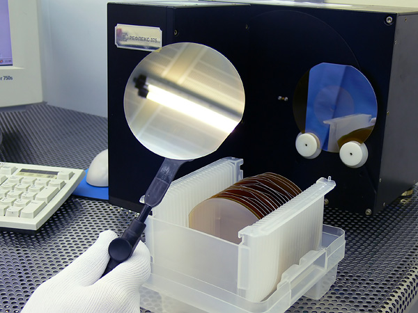
 Laboratory "Growth of semiconductor crystals" was founded in 1959, under the leadership of Academician M.S. Saidov, in the Physico-Technical Institute of the Academy of Sciences of the Uzbekistan. In the laboratory research works are carried out to study the physical and chemical foundations of technology for obtaining of semiconductor materials and devices based on them.
The main tasks are the establishment of regularities of interaction and the distribution of chemical elements in multicomponent one- and two-phase systems, applied to semiconductor materials science and solid state electronics, especially solar cells and LEDs.
The main direction of laboratory research is explanation of the physico-technological features of the synthesis of new solid solutions, models of self-organization in two and multicomponent solid solutions, obtaining nano-, homo- and heterostructures on the basis of elementary semiconductors and semiconductor compounds of class AIIIBV and AIIBVI on silicon substrates, and also the study of photovoltaic, thermal-voltaic, photothermal-voltaic and radiation effects in them.
Now, 5 doctors of sciences, 5 PhD, 2 candidates, 2 doctoral students, laboratory technicians and technicians have been working in the laboratory.
The main achievements of the laboratory.
In the laboratory new directions of research of semiconductor materials and converters of radiant and thermal energy into electrical were founded:1) a continuous solid solutions of semiconductor compounds; 2) impurity photovoltaics.
For the first time, based on the opening of a new phenomenon - the formation of new solid solutions, due to the replacement by molecules of elementary semiconductors of the IV group of molecules of semiconductor compounds from group III-V and II-VI and a number of theoretical and experimental studies, have developed three concepts for the development of solid solutions and impurity effects in them: 1) About existence of a new class of semiconductor continuous substitutional solid solutions and the prospects for their application; 2) About ways to implementation of impurity photovoltaic and photothermal and thermal effects in photo- and thermal elements, in order to significant increase in the efficiency of solar cells and thermo-photovoltaic systems.
To develop the concept of the existence of a new class of semiconductor substitutional solid solutions are advanced the following ideas: molecular elements C2, Si2, Ge2, Sn2, their combinations CGe, CSn, SiGeSiSn, GeSn and their more complex combinations are new, previously unknown chemical compounds, not described by traditional state diagrams, new chemical compounds of elementary semiconductors and binary compounds III-V, II-VI in liquid metallic solvents at a temperature below the melting point in the form of molecules and form substitutional solid solutions for low-temperature crystallization of epitaxial layers from the liquid phase.
A formula is proposed for the solubility of various elements in multicomponent systems and formulated the conditions for the formation of new substitutional solid solutions, which consist in the equality of the sums of valences and close values of the sums of the covalent radius of the atoms, forming molecules of solution-forming components.
Under the leadership of professor A.S. Saidov synthesized new class of semiconductor continuously graded band gap solid solutions on silicon substrates: 1st – class: IV1-xIVx: Si1-xGex, Si1-xSnx, Ge1-xSnx; 2nd – class: (IV2)1-x(AIIIBV)x: (Ge2)1-x(GaAs)x, (Si2)1-x(GaP)x, (Ge2)1-x(InP)x, (Sn2)1-x(InSb)x, (Si2)1-x(GaSb)x; 3rd – class: (IV2)1-x(AIIBVI)x: (Ge2)1-x(CdTe)x, (Ge2)1-x(ZnSe)x, (Si2)1-x(ZnS)x, (Si2)1-x(CdS)x, (Si2)1-x(ZnSe)x; 4th–class: (IV2)1-x-y(AIIIBV)x(AIIBV)y: (Ge2)1-x-y(GaAs)x(ZnSe)y, (Si2)1-x-y(ZnSe)x(GaP)y.
The conception of the ways of impurity photo- and photo-thermal-voltaic ef-fects is based on ideas on the expediency of using isovalent impurity elements and compounds, which satisfying the conditions for the formation of solid solutions of molecular substitution based on base semiconductors. A mechanism of the photo-voltaic effect is proposed, caused by isovalent impurities, which energy levels are in the valence band.
For the first time, detected the energy levels of molecules (Si2, Ge2, GaP) narrow-gap semiconductors, located within the forbidden band of wide band gap semiconductors of compounds AIIIBV and AIIBVI, and also the levels of molecules (GaAs, CdS, ZnSe) of wide band gap semiconductors inside the valence band of a narrow band gap semiconductor.
For the first time, detected by two-color emission diode heterostructures nGaP-n+(ZnSe)1-x-y(Si2)x(GaP)y (0<х<0.03, 0<y<0.09), due to electronic transitions with participation of molecular levels of Si2 (red light) and GaP (yellow light) with energy levels of 1.63 eV and 2.2 eV, respectively, located in the forbidden band of the solid solution (ZnSe)1-x-y(Si2)x(GaP)y.
For the first time, observed the thermal-voltaic effect in silicon, obtained by repeated re-melting of technical silicon in a solar furnace and in the graded band gap Si1-xGex solid solutions, which consists in the generation of current and voltage during a homogeneous heating of a sample with ohmic contacts.
For the first time, was observed the photo thermal-voltaic effect in nSi-p(Si2)1-x-y (Ge2)x (GaAs)y, pSi-n +(ZnSe)1-x-y (Si2)x (GaP)y heterostructures, consisting in the generation of current and voltage at combination photo and heat of carrier current generation under solar radiations.
For the first time, on the basis of the developed ideas about the possibility of self-organization process of defects in semiconductors of group III-V, the thermal-voltaic effect in these materials was observed.
For the first time, white luminescence was detected in nSi-pCdiamond, nSiC-pCdiamond heterostructures without a luminophore.
For the first time, polycrystalline silicon with a purity of 99.9 atomic % was obtained by an ecologically clean method in a small solar furnace with an eightfold re-melting of metallurgical silicon with a purity of 96 atomic% in the open air.
The laboratory prepared 8 doctors of sciences, including 1 academician of the Academy of Sciences of Uzbekistan, 3 laureate of the State Prize of the Republic of Uzbekistan, 27 PhD.
Phone: +99871 235 93 61
Fax: +998712354291
E-mail: ftikans@uzsci.net
Adress: Uzbekistan, 100084, Tashkent city, st. Chingiz Aytmatov 2B